Hardware
Warning
Documentation in progress...
Introduction
As mentioned in the requirements, the hardware design must be simple, small and robust. This will be kept in mind throughout the design.
This document will be split into sections for:
- Schematic
- Part selection
- Stackup
- Layout
- Manufacture
Schematic
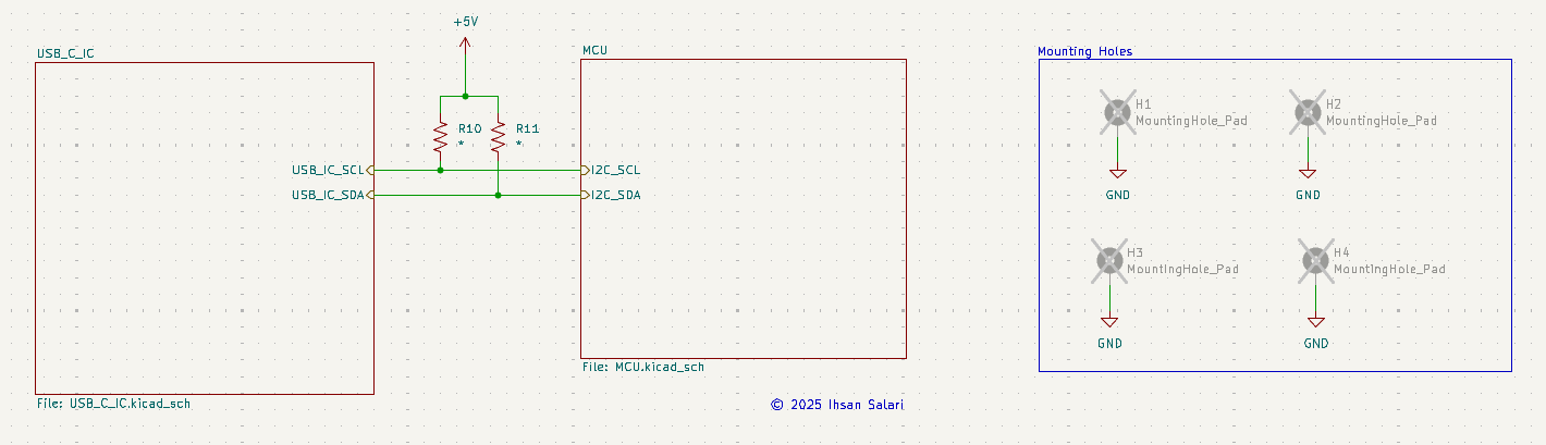
The high level schematic of the design consists of two modules. The first is the USB-C PD negotiation circuitry and the second is the MCU which sets desired output levels and communicates with the user.
PD Controller
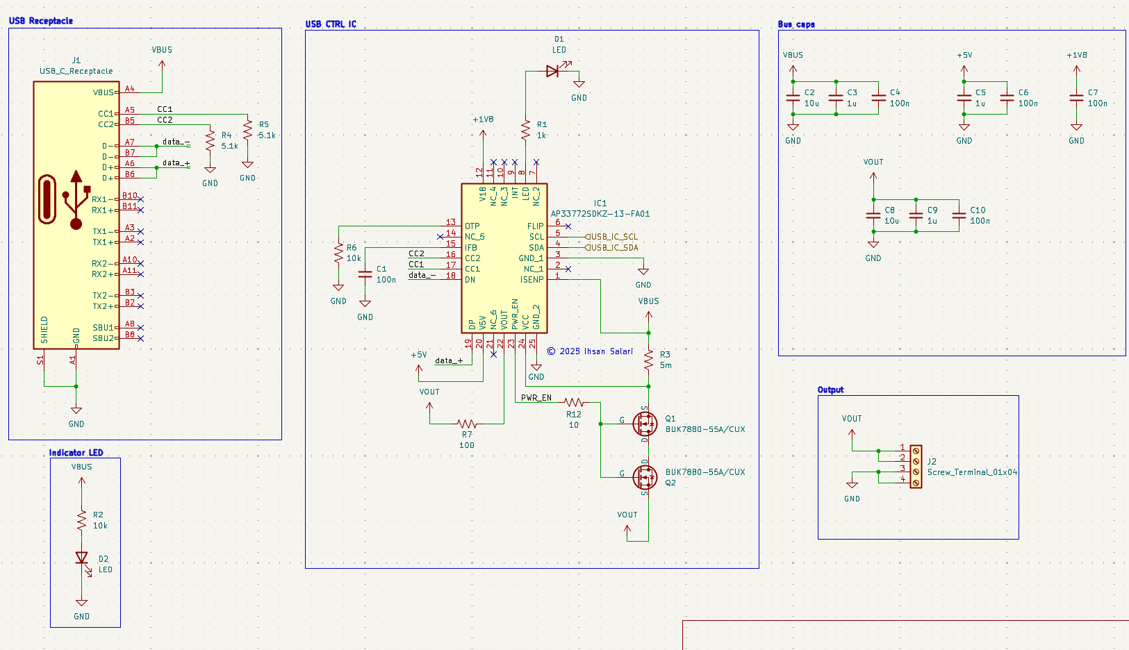
The PD controller chosen is the AP33772S. The required supporting componets include:
- MOSFETs to turn the output on/off,
- a USB-C receptacle,
- current sense resistor,
- and status LED with pre-programmed modes detailed in the datasheet.
The bus is also fitted with a status. This allows the user to roughly gauge bus voltage based on LED brightness.
The remaining passives either decouple the IC or serve another purpose detailed in the datasheet.
MCU
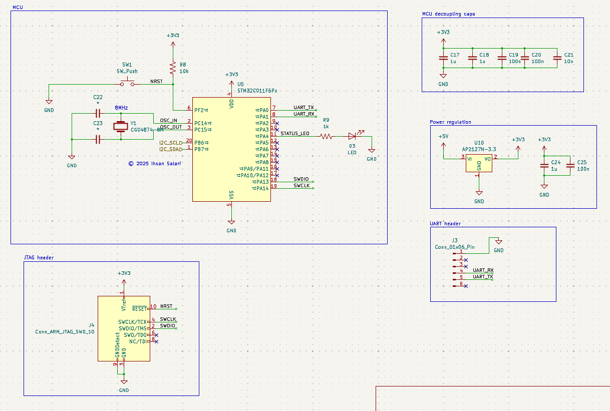
The chosen MCU is an STM32C0. Specifics of the part selection is detailed below.
The design includes:
- a heartbeat LED is added for simple status indication,
- a SW interface on JTAG header for easy programming,
- UART header for debug and user voltage selection,
- and a 3V3 linear regulator to supply power to the MCU from the PD controller's 5V rail.
The rest of the passives serve trivial decoupling or other purposes. See part selection for more details.
Part Selection
PD Controller
The AP33772S was chosen for it's simple I2C communication and ease of use. It is quite new, which means it supports many of the new PD features such as PPS and EPR. It's package is also quite small which is advantageous. It's older sibling, the AP33771 has been around for some time and was a good indicator that this new product would also succeed. The AP33772S is also used on some other comercial PD controllers, which indicated viability. Overall, this controller was chosen to ensure compatability with newest PD sources and ease of use at a relatively low cost of CAD $2.41.
MCU
The STM32C011F6P6 was chosen primarly for it's small TSSOP-20 footprint and low cost of CAD $1.46. The MCU needs to communicate with the PD controller and handle UART communication with the user. It must then reconcile presets, UART requests, and source capabilities to select the appropriate power mode. This can be achieved efficiently in firmware and is estimated to require no more than 32kB of flash memory.
MOSFETs
Due to the project timeline, these MOSFETs were chosen as a small enough solution in a package that is readily available, should it be necessary to replace it with a different part. This would come in handy later... Otherwise, the MOSFETs were spec'ed to match the PD controller datasheet. Not much to report on this.
Crystal
The MCU crystal was selected to have a resonant frequency of 8MHz. This speed is adequate for the tasks the MCU needs to accomplish, as none of these tasks are time-critical.
The capacitors accompanying the crystal were selected to be COG for temperature and clock stability, and their value was calculated by means of widely used rule of thumb.
Linear regulator
A generic 3V3 linear regulator was selected for the conversion from 5V to 3V3 for the STM32. The bus voltage is stepped down to 5V by the PD controller IC.
USB-C receptacle and screw terminals
The terminals were selected to be robust. Hence, a USB-C receptacle with many soldered body attachment legs was selected and a large screw terminal large enough for thick 5A-carrying wires was selected.
Passives
All passives were chosen to be 0603 as a nice tradeoff between size and ease of hand-rework. As I get better, I will shift to 0402, and later 0201? X7R and X5R caps were selected. Resistors with varying tolerance were selected depending on how critical accuracy is. For example, current sense resistor was selected to be \(5m\Omega\) with a 1% tolerance.
Nothing special for the rest of the components. Selected with a mix of low cost, quick selection for quick build turnaround, and small size.
Decoupling
Decoupling capacitors of various sizes are added in order to filter various frequencies. Smallest caps handle high frequencies, while the bigger ones serve as a capacitor bank and stabilize against sudden current draws.
Stackup
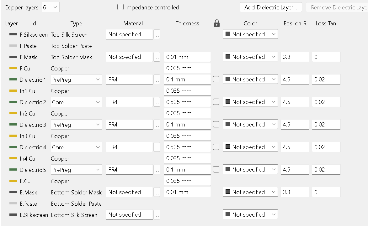
There are a few reasons to choose a multi-layer board over 2 layers. + First, the USB-C receptacle is quite small and there is not enough space on the top and bottom layers to route high current traces. + Second, the board can be made smaller by stacking power traces as opposed to making them wider. + Third, more copper directly around heat-producing components can improve heat dissipation.
The chosen stackup is as follows:
1. Sig/PWR
2. Sig/PWR/partial GND pour
3. PWR/GND
4. GND
5. PWR/GND
6. GND/some power
Layout
Overall considerations
As mentioned in the previous section, the layout is quite important for the power traces. Two main considerations were critical:
1. Ensure the power traces are able to handle the highest current (5A).
2. Ensure adequate return path to the USB-C adapter.
The later is not as important as it is a DC signal and there is no switching involved, but it is good practice and can prevent unwanted parts of the board from getting too hot due to currents flowing in the wrong places.
Reference images
Below are images of the layers in order from top to bottom.


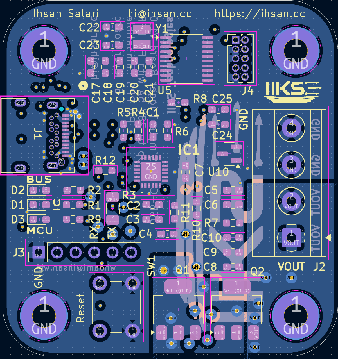
Specific layout choices
High level layout
I chose to keep the power path and digital circuitry on separate parts of the board. This has several purposes, the most important of which are:
+ keeping the hot components on one side, away from the ICs.
+ simpler debugging.
Component placement
- The PD controller was placed in the center as it has both connections to the power path and MCU.
- USB-C and screw terminal are place opposite one another. This allows for use in "inline" setups where the power comes in one side and exits the other. This can be more universal and more stable if attached to a free standing project.
- Mounting holes added all four corners for diverse mounting possibilities and stability.
- MCU placed far from power path to prevent thermal issues with heat produced by high currents.
- Staus LEDs placed near USB-C plug for convenient monitoring when plugging in.
- Decoupling capacitors are placed as close as possible to ICs with the smallest, high frequency filtering caps nearest to the IC.
- Crystal placed as close and centered as possible on the MCU pins.
It is important to note that no components were placed on the bottom side of the board. This was done to: + simplify the assembly process using a hot plate to reflow the PCB. + Also, this would allow the board to sit more flat on a surface. + Finally, the assembly process is simpler if minimal components need to be soldered on as opposed to reflowed. Given my current hot-plate reflow setup, I can only reflow one side of the circuit board.